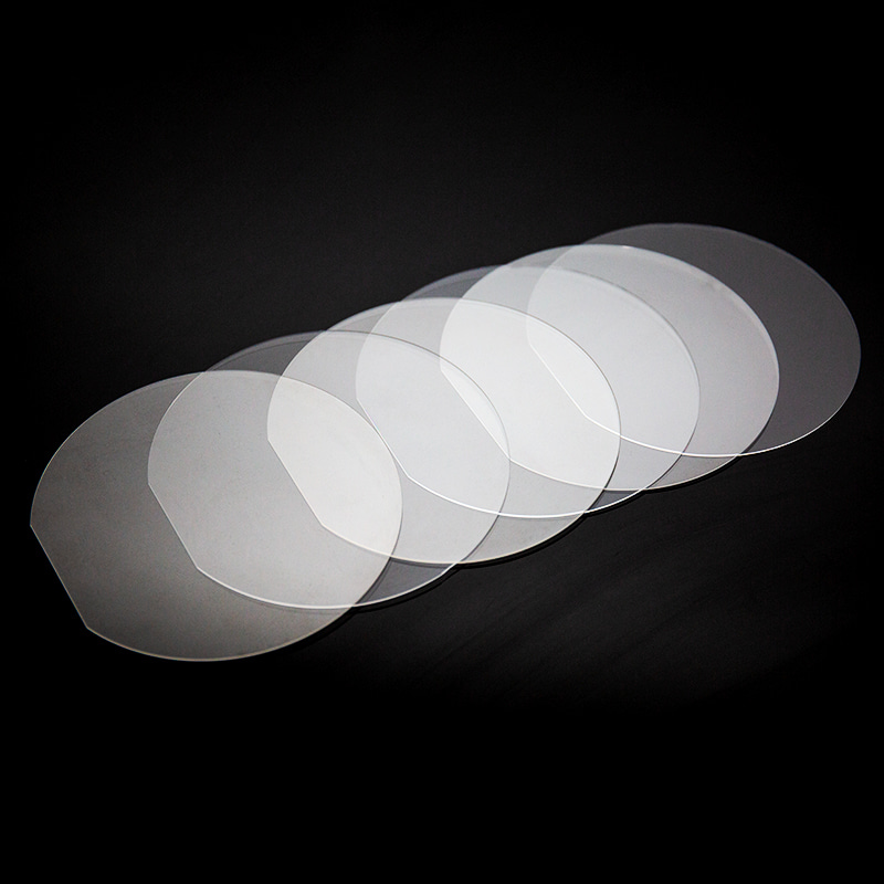
In the age of advanced imaging technologies, where clarity and precision are paramount, optical wafers play a crucial role in the performance of optical sensors. Whether in smartphones, medical imaging devices, or industrial cameras, the quality of these wafers directly influences the effectiveness of imaging systems. But what exactly are optical wafers, and how do they enhance the performance of optical sensors? Let’s unpack this intricate relationship and explore how these vital components contribute to imaging quality.
Understanding Optical Wafers
Optical wafers are thin slices of material, often silicon or glass, that have been meticulously crafted to manipulate light. These wafers serve as the foundation for various optical components, including lenses, mirrors, and sensors. The precision in manufacturing these wafers—often to within a few nanometers—ensures that they can guide and focus light effectively, minimizing distortions and maximizing image clarity.
The material properties of optical wafers, such as refractive index and surface smoothness, are critical. For instance, high-quality optical glass can transmit light with minimal absorption and scattering, which is essential for high-resolution imaging. As technology advances, the development of new materials, like low-dispersion glass, further enhances the capabilities of optical sensors.

Enhancing Sensitivity and Resolution
Optical sensors rely on the accurate detection of light to create images, and the quality of the optical wafer is instrumental in this process. A high-quality wafer can significantly improve the sensitivity of the sensor, enabling it to detect faint light signals that lower-quality wafers might miss. This is particularly important in applications like astrophotography or medical diagnostics, where the ability to capture subtle light variations can lead to better image interpretation.
Moreover, the resolution of imaging systems is directly tied to the optical wafers used. When light passes through a well-crafted optical wafer, it experiences minimal aberrations, allowing for sharper and more detailed images. Research indicates that imaging systems utilizing superior optical wafers can achieve resolutions that are up to 30% better than those using standard wafers. This level of detail is crucial in fields like microscopy or surveillance, where every pixel counts.
The Future of Optical Wafers in Imaging Technology
As the demand for more advanced imaging systems grows, so does the innovation surrounding optical wafers. Emerging technologies like adaptive optics and augmented reality are pushing the boundaries of what optical sensors can achieve. For instance, adaptive optics systems utilize deformable mirrors made from optical wafers to correct distortions in real-time, resulting in exceptionally clear images.
Furthermore, the integration of artificial intelligence in imaging systems is leading to smarter optical sensors that can adjust their settings based on the quality of the optical wafer. This synergy can enhance performance in various lighting conditions, making imaging systems more versatile and efficient.
Optical wafers are not just passive components; they are the backbone of high-performance optical sensors in imaging systems. Their ability to manipulate light with precision translates into improved sensitivity, resolution, and overall image quality. As technology continues to advance, the role of optical wafers will undoubtedly evolve, paving the way for even more sophisticated imaging applications. For anyone invested in the future of imaging technology, understanding optical wafers is essential—a small slice of material that makes a big difference in the world of optics!

 English
 日本語
日本語 русский
 Español
 Deutsch
 中文简体
中文简体


 苏公网安备32041102000130号